3mil Line 1.6mm Thickness Single Layer 350um HASL PCB Electronic Board
| Item | Spec |
| Layers | 1~20 |
| Board Thickness | 0.1mm-8.0mm |
| Material | FR-4, CEM-1/CEM-3, PI, High Tg, Rogers, PTEF, Alu/Cu Base, etc |
| Max Panel Size | 600mm×1200mm |
| Min Hole Size | 0.1mm |
| Min Line Width/Space | 3mil(0.075mm) |
| Board Outline Tolerance | 士0.10mm |
| Insulation Layer Thickness | 0.075mm--5.00mm |
| Out Layer Copper Thickness | 18um--350um |
| Drilling Hole (Mechanical) | 17um--175um |
| Finish Hole (Mechanical) | 0.10mm--6.30mm |
| Diameter Tolerance (Mechanical) | 0.05mm |
| Registration (Mechanical) | 0.075mm |
| Aspect Ratio | 16:01 |
| Solder Mask Type | LPI |
| SMT Mini. Solder Mask Width | 0.075mm |
| Mini. Solder Mask Clearance | 0.05mm |
| Plug Hole Diameter | 0.25mm--0.60mm |
| Impedance Control Tolerance | 士10% |
| Surface finish | ENIG, OSP, HASL, Chem. Tin/Sn, Flash Gold |
| Soldermask | Green/Yellow/Black/White/Red/Blue |
| Silkscreen | Red/Yellow/Black/White |
| Certificate | UL, ISO 9001, ISO14001, IATF16949 |
| Special Request | Blind hole, Gold finger, BGA, Carbon ink, peelable mask, VIP process, Edge plating, Half holes |
| Material Suppliers | Shengyi, ITEQ, Taiyo, etc. |
| Common Package | Vacuum+Carton |


Product Details:
1. Single, Double side & Multi-layer PCB.
2. Buried/Blind Vias, Via in Pad, Counter Sink Hole, Screw Hole(Counterbore), Press-fit, Half Hole.
3. HASL lead-free, Immersion Gold/ Silver/Tin, OSP, Gold plating/finger, Peelable mask,
4. Printed Circuit Boards adhere to IPC Class 2 & 3 international PCB standard.
5. Quantities range from prototype to medium&big batch production.
6.100% E-Test


ABIS Circuits Co., Ltd established in 2006, Located in Shenzhen, our company has about 1100 workers and two PCB workshops with about 50000 square meters.
Now we have passed ISO9001, ISO14001, UL, etc., With constant hard work of our staff and ongoing support from customers both home and abroad, we can provide up to 20 layers, Blind and buried Board, high-precision(Rogers), High TG, Alu-base and flexible boards to our customer with fast turn and high-quality level.
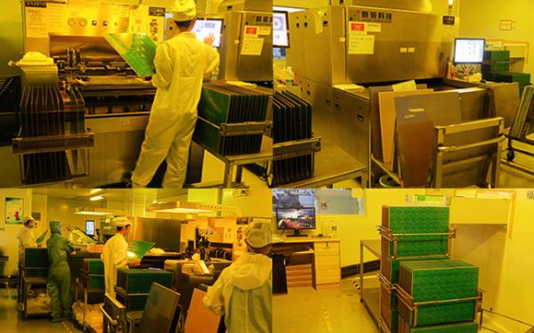
Workshoop:


Q1: What files do you use in PCB and assembly Quotation?
A1: Gerber, pcb. Auto CAD + Bill of Material
Q2: How do you make sure the quality?
A2: Our Product is all 100% tested including Flying Probe Test (for sample), E-test (mass) or AOI.
Q3: Can we visit your company?
A3: Of course! Welcome to visit our company,Abis is located in Shenzhen, Guandong province, China.
Q4: What is the lead time?
A4: It takes 3-5 working days for sample, 7-10 working days for batch production based on files and quantity.
Q5: Will you keep our information and files secret?
A5: Sure! It is our basic principle to keep business secrets to protect our customers' rights and behalf.
Q6. How to work with you?
A6: -Email and send us the PCB layout file, BOM list
- We will provide reply confirmation within 12 hours and reply to the offer within 3-5 days.
- Waiting for your company to confirm the price, order and payment method.
- We will start the production.
Product Tags:

|
|
3mil Line 1.6mm Thickness Single Layer 350um HASL PCB Electronic Board Images
|